With more and more data comes the need for storage and fast access which means that technology like DDR5 has never been more important.
 How Does the New Generation Memory – DDR5 – Change Things?

Article from | Tektronix
From augmented reality to artificial intelligence, cloud computing to IoT, 5G is fueling growth in new technologies – and the data they create. With more and more data comes the need for storage and fast access which means that technology like DDR5 has never been more important. The need for data centers to continuously store, transfer and process this data pushes the limits of high-speed signaling and ushers in testing challenges not seen in memory to date.
What’s Changed?
DDR5 is very different from DDR4 and is actually more like LPDDR4. Check out these nine changes that DDR5 brings to the table:
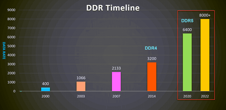
- It’s faster! First and foremost, data rate goes up to 6.4 Gbps, whereas DDR4 stopped at 3.2Gbps. There's also a provision in the spec to push the speed limit beyond 8 Gbps in the coming years. The channel structure is similar to LPDDR4, where we have two independent 40 bit channels with ECC. We also have higher prefetch, higher burst length and increased bank groups. This is all to increase the efficiency and enable high-speed modes.
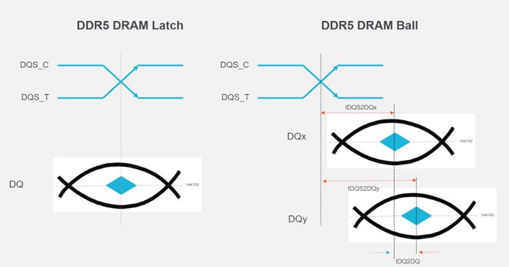
- Another big change in DDR5 is that writes are not center aligned. There's a fixed offset between DQS and DQ. What that means is we cannot just measure the delay between DQS and DQ on the scope and figure out whether it's read or write. That luxury is gone. Read-Write burst separation is all set to be more complicated.
- New clock jitter measurements. DDR5 introduces Rj, Dj and Tj measurements in place of period and cycle to cycle jitter measurements. Specs of Rj are very tight at the max data rate. Good signal integrity will be paramount to measure these parameters with confidence.
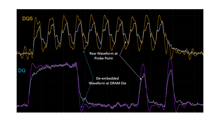
- De-embedding is going to be critical at higher DDR5 data rates. De-embedding is a technique to remove the probe and interposer loading. It is also used to move the probe point virtually from DRAM ball to the DRAM die to minimize reflections. We want to see what the Rx is seeing. To successfully create de-embedding filter files or transfer function, s-par files are required – lots of them. Idea is to mimic the DDR channel as faithfully as possible by using s-par models for SOC package, board models, DRAM package, interposers, probes as well as IO settings like Tx drive strength and Rx ODT (if applicable). In the absence of s-par models, one can also use simple transmission line parameters like propagation delay and characteristic impedance by measuring the reflection on the scope screen.
- For the first time we will have Rx equalization, 4-Tap DFE, in the receiver. The increase in the data rate in DDR5 is achieved without moving the DQ bus to differential signaling i.e. the DQ bus is still single-ended – same as DDR3/4. However, memory channel has lots of impedance mismatched points which increases the overall ISI due to reflections. At data rates above 4800 Mbps, the data eye at the DRAM ball is expected to be closed. A 4-tap DFE is implemented in the DDR5 DRAM Rx to help equalize the DQ signals and open the data eyes after the data is latched by the receiver. Furthermore, RCD’s CA Rx will also need DFE to ensure reliable signal capture.
- Another dramatic change for DDR5 is the inclusion of a loop back channel. If you look at the pin map of DDR5, you will find dedicated DQS/DQ loop back pins. This will be used to enable standalone DRAM RX/TX characterization. A loop back channel is critical. In fact, it is how we know what bit decision a receiver actually makes in real time. It's a single wire that's shared between all the different receivers, and because it has poor signal integrity and for that and other reasons, it's why we only send back every fourth bit or every second bit, so that there's plenty of time to be able to make sure that an outside receiver or bit error detector can check with 100% accuracy the quality of the on-die Rx.
- There is a need for standalone DRAM Rx/Tx testing in DDR5 using a BERT and/or a flexible pattern generator. This opens a whole new suite of tests including voltage & frequency sensitivity and stressed eye tests that were not present in DDR3/4. Concept is a simple one – anyone should be able to use the standardized JEDEC fixture, follow JEDEC defined test procedure and perform standard tests to determine the health of DRAM Rx/TX.
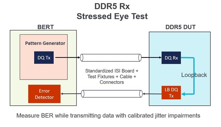
- Accurate stress calibrations are going to be a big issue in DDR5 RX testing, and that is getting accurate S-parameter models, both ones that you'll have to estimate as well as measure for all the segments. Another critical feature will be being able to make accurate or good guesses for the measurement depths and the oscilloscope record sizes, so that you're not wasting too much time.
- DRAM Rx/Tx testing will present a huge database management problem. Automating and managing the massive amounts of s-par files, de-embedding models, and measurement results is going to be a nightmare. Imagine testing 80+ pins at different speed grades for multiple DIMM configurations from different vendors. That's going to be very, very hard.
Compared to DDR3/4, DDR5 improves bandwidth, density, and channel efficiency. But higher data transfer rates and faster signal speeds require higher performance measurements for compliance, debugging and validation. Understanding the differences inherent in DDR5 can help with efficient verification and debugging.
To address these differences, and other thorny measurement challenges associated with the new DDR5 standard, check out the on-demand webinar – How to Solve 5 Key DDR5 Test Challenges for Next Gen Memory.
The content & opinions in this article are the author’s and do not necessarily represent the views of ManufacturingTomorrow
Comments (0)
This post does not have any comments. Be the first to leave a comment below.
Featured Product

